
As part of today’s headline Computex keynote, NVIDIA announced a new member in their suite of NVLink interconnect technologies: NVLink Fusion. And this latest entry may be the most interesting yet, as NVIDIA is taking a big step towards opening up the NVLink ecosystem to third-party CPUs and accelerators, releasing IP and hardware designed to facilitate third-party designs interoperating with NVIDIA’s own silicon over NVLink connections. The end result isn’t quite a true mix-and-match ecosystem – no matter what, you still need some NVIDIA silicon in there – but the intention is to let NVIDIA’s partners start building what are essentially semi-custom racks mixing NVIDIA and custom chips.
Even before NVIDIA acquired network hardware manufacturer Mellanox, the company has been developing its own local networking and interconnect technologies with its short-reach NVLink standard. First introduced with its circa-2016 Pascal, NVLink was used as an alternative to PCI-Express as a faster cache-coherent interconnect between GPUs. In the intervening years, NVIDIA has ramped up the bandwidth of NVLInk significantly while also expanding its reach with NVLink switches, and the ability to use it to electrically connect with neighboring nods in a rack. These days, NVIDIA considers NVLink one of their most important technologies, as it has allowed them to address the challenges of scaling-up a GPU system to the size of a whole rack, making their 72 GPU NVL72 racks possible.
Now NVIDIA is looking to take the next step with its NVLink technology and address customer flexibility needs by opening it up to semi-custom designs. Whereas the current use cases for NVLink are all pure NVIDIA systems – primarily their Grace Hopper and Grace Blackwell CPU+GPU configurations – NVIDIA will be opening up the NVLink ecosystem for semi-custom designs, allowing system vendors to either swap out the NVIDIA CPU or NVIDIA GPU for custom hardware. The technology is aptly being named NVLink Fusion, describing how it will allow third-party silicon to be fused into NVLink networks.

NVLink Fusion CPU: Using C2C to Connect Custom CPUs to NVIDIA GPUs
Diving under the hood, there are essentially two different technologies here that are being bundled under the single NVLink Fusion banner. First and foremost is semi-custom CPUs – allowing non-NVIDIA CPUs to connect to NVIDIA GPUs over NVLink’s short-range chip-to-chip variant, NVLink C2C. Strictly speaking, this part of NVIDIA’s announcement isn’t new – the company opened up NVLink C2C for custom silicon integration back at GTC 2022, so this is the next step of that program. Thus far we haven’t seen any (publicly announced) third-party chips released that support NVLink C2C under this existing program, but with that said, the development cycle for such hardware would take years, meaning that the first wave of NVLink Fusion-capable CPUs may have been started under the older program.
Either way, NVIDIA is back with a fresh effort to promote using NVLink C2C with third-party CPUs under the NVLink Fusion branding. Overall, this technology is relatively straightforward, with hardware vendors licensing the NVLink C2C technology and integrating it into their chips to allow them to connect to NVIDIA GPUs. These semi-custom chips would essentially replace the Grace CPUs in current GB200/GB300 designs, with the semi-custom CPU taking on Grace’s job. Previously the only way to pair up an NVIDIA datacenter-class GPU was to use the PCIe variants of those cards (which have seemingly gone away entirely), so this is in effect the next iteration of those kinds of mixed-vendor systems.

NVLink Fusion GPU: Using Chiplets to Add NVLink 5 to Custom Accelerators
The more interesting and novel aspect of the NVLink Fusion announcement – and the portion requiring new NVIDIA hardware – is using NVLink Fusion to pair up NVIDIA CPUs with third-party GPUs and accelerators. This is currently impossible on multiple levels: not only are there no NVLink C2C-enabled accelerators that can hook back to Grace other than NVIDIA’s own Hopper and Blackwell GPUs, but those GPUs are also where the full-featured NVLink 5 PHYs are that allow Grace Hopper and Grace Blackwell nodes to connect to an NVLink network. In short, it’s never been possible to even plug a third-party accelerator into an NVLink network, never mind plugging a Grace CPU into all of that.
To that end, NVIDIA is getting into the chiplet game. The company has developed an NVLink 5 chiplet that is designed to be integrated into semi-custom accelerator designs, allowing those accelerators to gain NVLink 5 functionality by going through NVIDIA’s chiplet. Notably here, NVIDIA is not licensing NVLink 5 for third parties to implement; NVIDIA’s high-bandwidth interconnect technology is remaining proprietary. But in the spirit of mix-and-matching chiplets to build larger processors, NVIDIA is giving chipmakers the means to add NVLink 5 by adding NVIDIA’s chiplet.
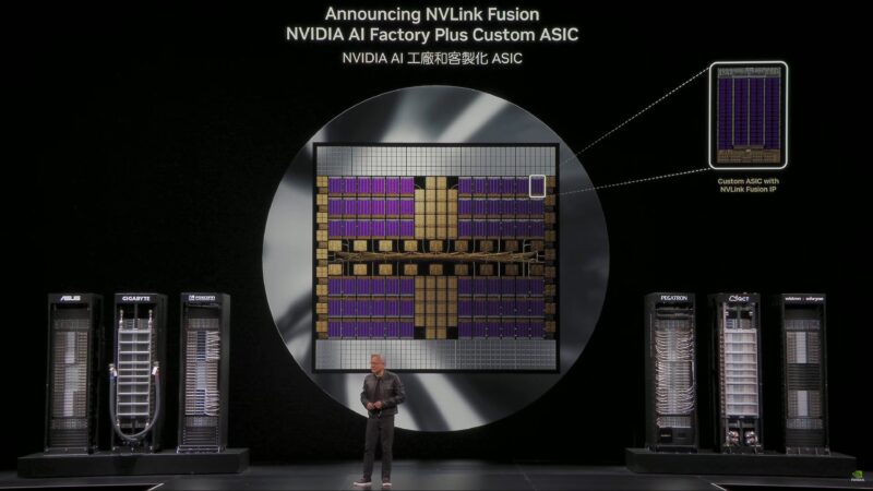
At this point NVIDIA is not offering any hardware specifications for the chiplet itself. So it’s unclear how big it is or how much power it may consume. Or, for that matter, how many NVLink lanes are available from a chiplet, and thus a semi-custom accelerator (will it comparable to a GB200 GPU?). And NVIDIA has not clarified what technology will be used to link up the NVLink chiplet to the rest of the accelerator – if it will be NVLink C2C (which is already needed for the CPU link), or if it will be another technology. Still, if you’re making a high-performance accelerator and wanted to plug it into an NVLink network, NVIDA is finally making that possible in a fashion.
But All Nodes Must Contain NVIDIA Hardware
Standards and topologies aside, NVIDIA has made it clear that NVLink Fusion will be treated like an either/or technology. That is, you can use it to integrate a semi-custom CPU or a semi-custom GPU, but not both. So system vendors will not be able to build NVLink-enabled systems using both third-party CPUs and third-party GPUs – they must still have a piece of NVIDIA silicon on their nodes.
At the moment, this seems to be strictly a licensing limitation rather than a technical limitation. Because all of the real heavy lifting for NVLink 5 is done by the GPU – be it an NVIDIA GPU or an accelerator with an NVLink Fusion chiplet – the CPU doesn’t hold a pivotal role in enabling NVLink 5 (and indeed, doesn’t even use it). But as NVIDIA is in the business of selling silicon, there’s no incentive for them to cut themselves out of future systems. Even offering chip designers the means to replace NVIDIA GPUs with third-party accelerators is relatively wild, as it’s NVIDIA’s GPUs that are driving most of the company’s fortunes right now.
Still, reading between the lines it sounds like NVIDIA’s partners have been pushing hard for some flexibility in their rack designs. Grace Blackwell is not a one-size-fits-all solution, especially as the future of AI accelerators is still far from clear. But whatever the reason, the end result is the same: NVIDIA is finally opening up NVLink to outside companies – at least a little bit.

For now, the immediate beneficiaries of this will be Alchip, AsteraLabs, Marvell, and MediaTek, all of whom have confirmed that they’re working on their own accelerators or helping to build accelerators that will incorporate NVLink Fusion. Meanwhile both Fujitsu and Qualcomm have confirmed that they are working on new NVLink Fusion-capable CPUs that can be paired with NVIDIA’s GPUs. This includes Fujitsu’s next-generation high-end Armv9 processor, Monaka, as well as Qualcomm’s unnamed upcoming data center CPU. In both cases, the CPU vendors are looking to drive further efficiency, with NVLink Fusion giving them the means to plug in to NVIDIA’s GPUs and their high-performance NVLink networking architecture.
Meanwhile, Cadence and Synopsys are both participating in the NVLink Fusion program as technology partners as well, making their IP blocks and design services available to companies who are looking to build their own NVLink Fusion-capable hardware.


The thing with NVlink is that it is coherent so that there is data synchronizations happening. While the NVlink higher protocol and PHY are handled by the chiplet, there likely needs to be some sort of egress protocol to maintain coherency with any custom silicon.
What would have been really impressive is if this NVlink chiplet that can be licensed was photonics based (or was two chiplets with protocol + photonics PHY) to really scale things up. This will likely happen at a later generation but would’ve really kicked off adoption with a bleeding edge implementation.
Having said that, I am surprised about how much they emphasized copper for data in their current topologies. I was not expecting so much detail into the spine for a keynote since if you break it down a very large controlled rat’s nest of wires.
Other thing about the keynote I found disappointing is the mention of a 5 year road map at the start of the presentation and no mention of it later. The points of becoming an infrastructure company still stand though.